Defect location and class
bright-field and dark-field inspection
Material Analysis · Microscopy & Imaging
Characterise defect location and class, feature dimensions and placement, and wafer-level yield and spatial defect distribution using a scope agreed around your sample and decision.
Why this test
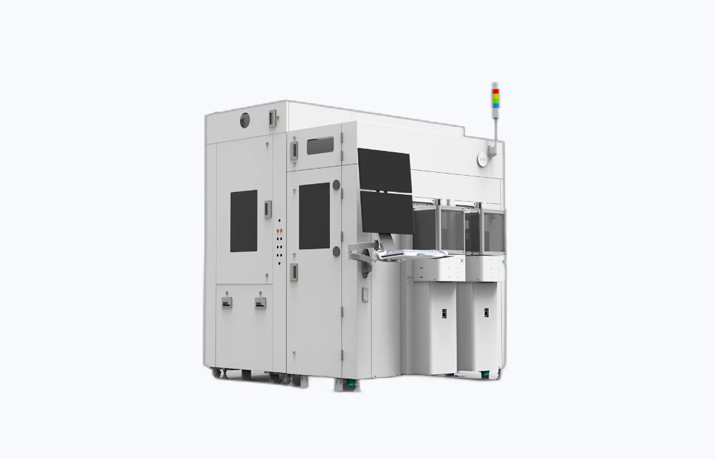
Micro-LED Wafer AOI Inspection is selected when the project needs defensible information on defect location and class, feature dimensions and placement, or wafer-level yield and spatial defect distribution. Automated…
bright-field and dark-field inspection
multi-wavelength imaging
recipe development and automated classification
Choose the scope
The measurement mode, preparation route and reporting depth depend on what you need to learn from the sample.
defect location and class
feature dimensions and placement
wafer-level yield and spatial defect distribution
Common outputs
Fields, measurement conditions, processing and file formats are confirmed before work begins.
Wafer defect map reported with the agreed units, sample reference and measurement conditions.
Classified defect image set supplied in a labelled format suitable for direct sample or condition comparison.
Yield and defect statistics provided with the processing basis and quality checks agreed during technical review.
Method-specific images included when selected in the confirmed reporting scope.
Sample requirements
Provide representative, clearly labelled samples and identify the region, feature or comparison that matters.
| Suitable sample or input | Submission requirement | Planning note |
|---|---|---|
| Powder / particles | Provide a dry, homogeneous and clearly labelled sample in a sealed container. | Exact mass and any drying or dispersion step are confirmed after technical review. |
| Film / coating | Provide the coated substrate or a flat film with the test surface and coating side clearly marked. | State the substrate, nominal thickness and whether sectioning or mounting is permitted. |
Region of interest: include a marked image, sketch or reference when the target feature is localised.
Handling: declare hazardous, magnetic, volatile, moisture-sensitive, beam-sensitive or temperature-controlled material before dispatch.
Questions and answers
Short answers to issues that can change preparation, scope or interpretation.
Provide powder / particles, film / coating as applicable. Exact quantity, dimensions and preparation are confirmed during technical review.
Choose the mode around the decision you need to make. For defect location and class, start with bright-field and dark-field inspection; add multi-wavelength imaging when comparison or quantification is required.
Typical turnaround is 7 working days after sample acceptance and method confirmation.
Optical AOI may not identify electrically inactive but visually normal devices. Classifier performance depends on representative training and acceptance criteria.
Configure the service
A £45 service fee applies to orders under £300, excluding VAT.
Typical turnaround: 7 working days
Configure & Book