Crystal orientation and texture
area map
Material Analysis · Microscopy & Imaging
Characterise crystal orientation and texture, grain size and boundary character, and phase distribution and local misorientation using a scope agreed around your sample and decision.
Why this test
Electron Backscatter Diffraction is selected when the project needs defensible information on crystal orientation and texture, grain size and boundary character, or phase distribution and local misorientation.…
area map
high-angular-resolution or transmission EBSD
EDS-EBSD phase correlation
Choose the scope
The measurement mode, preparation route and reporting depth depend on what you need to learn from the sample.
crystal orientation and texture
grain size and boundary character
phase distribution and local misorientation
Common outputs
Fields, measurement conditions, processing and file formats are confirmed before work begins.
Orientation and inverse-pole-figure maps supplied with the agreed units, labels, sample reference and measurement conditions.
Phase, grain, boundary, and misorientation statistics supplied with the agreed units, labels, sample reference and measurement conditions.
Indexed pattern quality and acquisition parameters supplied with the agreed units, labels, sample reference and measurement conditions.
Example results
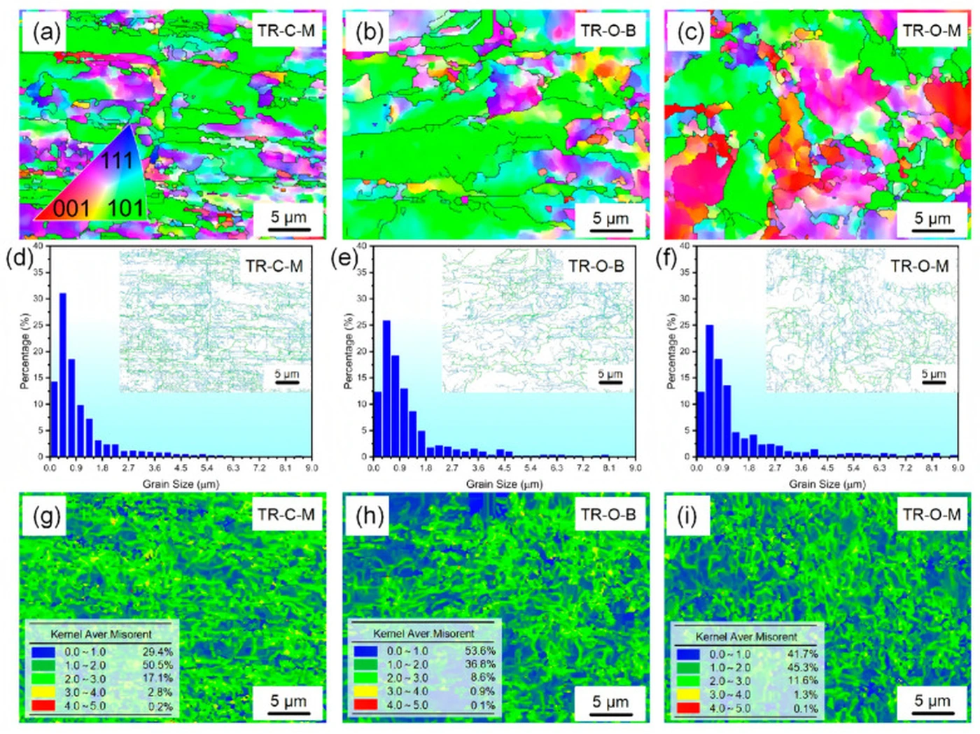
EBSD maps compare grain orientations, grain-size distributions and local misorientation across cold-rolled copper foil layers.
Tong Wu et al. · source · CC BY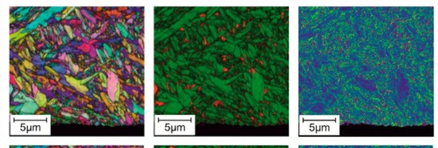
A coordinated EBSD row shows orientation, retained-austenite phase distribution and local misorientation in case-hardened gear steel.
Marina Knyazeva et al. · source · CC BYSample requirements
Provide representative, clearly labelled samples and identify the region, feature or comparison that matters.
| Suitable sample or input | Submission requirement | Planning note |
|---|---|---|
| Metals, ceramics, minerals, semiconductors, and crystalline coatings with polished surfaces | Provide a flat, deformation-free polished surface, preferably finished by electropolishing or ion milling where needed. State expected phases and the coordinate system for texture. Avoid coatings that obscure diffraction unless specifically agreed. | Surface preparation is critical and poorly diffracting or nanocrystalline regions may not index. |
Region of interest: include a marked image, sketch or reference when the target feature is localised.
Handling: declare hazardous, magnetic, volatile, moisture-sensitive, beam-sensitive or temperature-controlled material before dispatch.
Questions and answers
Short answers to issues that can change preparation, scope or interpretation.
Provide a flat, deformation-free polished surface, preferably finished by electropolishing or ion milling where needed. State expected phases and the coordinate system for texture. Exact quantity and preparation are confirmed after reviewing the material and objective.
Choose the mode around the decision you need to make. For crystal orientation and texture, start with area map; add high-angular-resolution or transmission EBSD when comparison or quantification is required.
Typical turnaround is 8–12 working days after sample acceptance and method confirmation.
Surface preparation is critical and poorly diffracting or nanocrystalline regions may not index. The result is surface- or section-specific.
Configure the service
A £45 service fee applies to orders under £300, excluding VAT.
Typical turnaround: 8–12 working days
Configure & Book