Atomic- or nanoscale surface topography
Assess atomic- or nanoscale surface topography as part of a lab-ready investigation scope.
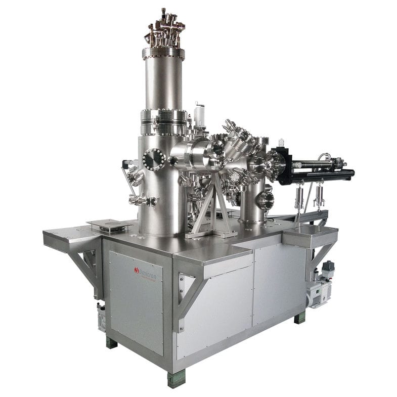
Material Testing · Microscopy & Imaging
Overview & applications
STM helps engineering and research teams investigate atomic- or nanoscale surface topography, surface defects, steps, terraces, and local electronic contrast, conductive surface behaviour under controlled imaging conditions with a lab-ready scope. TESTDOG can help translate an unclear request into the right imaging route, sample preparation notes and reporting requirements.
Use this page as a starting point for deciding whether STM is suitable before requesting a quotation.
Assess atomic- or nanoscale surface topography as part of a lab-ready investigation scope.
Assess surface defects, steps, terraces, and local electronic contrast as part of a lab-ready investigation scope.
Assess conductive surface behaviour under controlled imaging conditions as part of a lab-ready investigation scope.
Samples & requirements
Available options and related modes
Ambient STM can be scoped where the sample, objective and partner capability are suitable.
Conductive surface imaging can be scoped where the sample, objective and partner capability are suitable.
Atomic / nanoscale topography can be scoped where the sample, objective and partner capability are suitable.
SPM comparison with AFM can be scoped where the sample, objective and partner capability are suitable.
Deliverables
STM topography images.
Feature-height or profile information where requested.
Basic imaging notes.
Final deliverables depend on sample condition, selected mode, instrument access and the agreed reporting scope.